Scientists invent metamaterials which allow for semiconductor-free microelectronics.
Researchers have developed a new type of materials that will allow the creation of semiconductor-free microelectronics. This means that electronic devices, from phones, computer to solar panels will be more efficient in handling their power.
Silicon semiconductors have revolutionized technology by allowing manufacturers to install billions of transistors in chips the size of a few square inches. As great as they are, the technology does have some limits. For example, the velocity of electrons in the electric current that pass through them is limited by the resistance of the materials from which the semiconductors are made of. This requires a boost of energy to allow the electrons to cross the gap, which is created by silicon’s insulating properties.
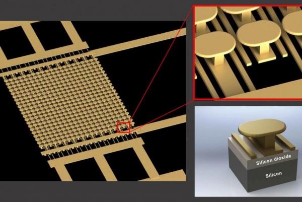
However, the new metamaterials invented by researchers at UC San Diego, are similar to old-school vacuum tubes because they use free electrons. The team of researchers solved the problem of electrons which require high voltage and high temperatures or a laser to release the electrons. They built a nanostructure from gold with additional gold strips parallel to it. It combines a low amount of voltage of only 10 volts with a low-powered laser to free the electrons from the gold.
Scientists discovered that this method led to 1000 percent increase in the conductivity of the entire system the metamaterial was used in. The change is high enough that it even allows the structure to maintain on and off states like an optical switch. The whole device can act as a transistor, power amplified or even a photodetector thanks to the metamaterials. The most amazing feature of this new invention is that it works with less resistance and even handle a much higher amount of power.
The research is still very much in its early stages. However, their findings, which were published in the journal Nature, represent a proof-of-concept. It can be used by the researchers to attract more research funds and further develop and improve their invention. Their next step is to determine how much can the metamaterials can be scaled without affecting their performance.
Its applications will lead to semiconductor-free microelectronics as well as photovoltaics, possibly weaponry and environmental applications. The research was funded by DARPA.
What do you think about the new discovery of metamaterials and semiconductor-free microelectronics?
Image credit: UC San Diego Applied Electromagnetics Group